I have built a circuit around 4 input signals from the pc
printer port.
D0 = enable charge transfer pulse frame 1
D1= enable charge transfer pulse frame 2
D2 = On chip amp enable.
D3 = Shutter enable.
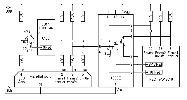
My
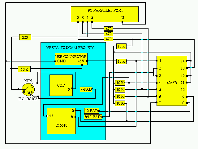
thanks to Jim Talbot for the graphic.
|
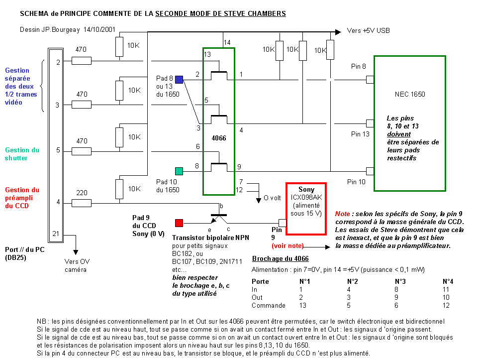
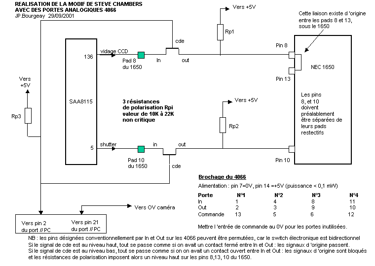
An graphic by Ashley Roeckelein is here
(Notes in French by Jean-Pierre Bourgeay here and
here)
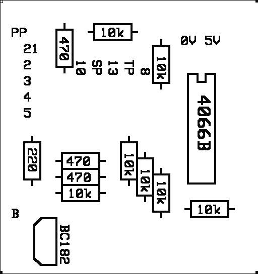
The design is pretty modular so you can
just connect up the bits you want. The chip I have built
the circuit around is the 4066. Jean-Pierre Bourgeay
introduced me to this chip with his simplification of the original circuit. I have chosen to keep
the 4 signals separate, as this will give the software
writers more flexibility. Firstly leads need to be
connected to the D16510 chip. I won't go into details
here as the connections are identical to the original mod
except that the connection between pins 8 and 13 needs to
be broken and connection made to each pin separately. The
modifications to the D16510 connections control all
features of the mod except the ccd amp.
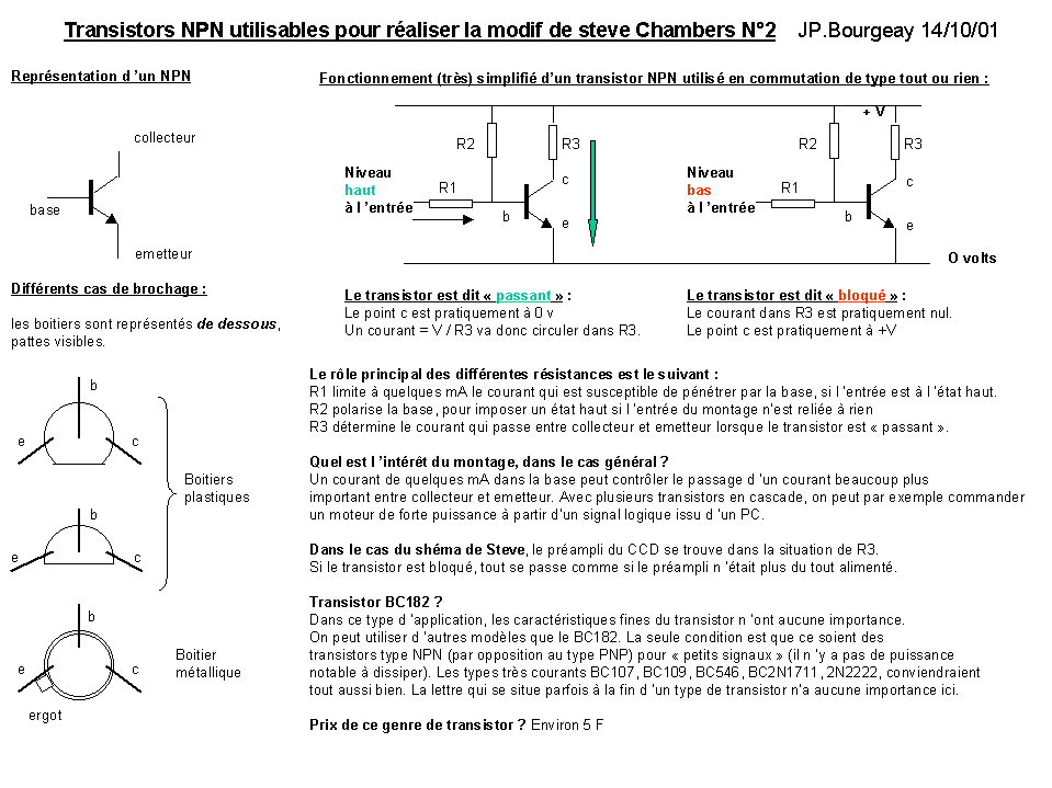
To allow the ccd pre amp to be powered off a transistor
is placed in series with pin 9 and its connection to
ground. This part of the mod is easier than the work
required to the d16510 chip but does carry a bigger risk
of destroying the camera. The pre amp is powered from a
'fragile' 15 v supply. This comes into the ccd on pin 8.
A couple of months ago I destroyed a ccd camera by
accidentally grounding this supply. If you want to learn
from my mistake, check very carefully connections you
make in this area before connecting the power.
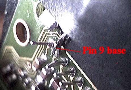 |
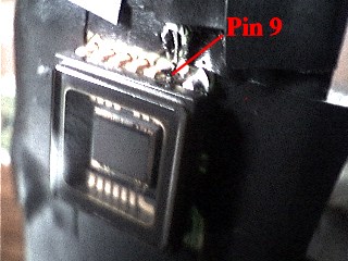
The end of pin 9 has been bent to aid soldering
The control transistor can be mounted next to the logic
chip and control the amp via flying leads but beware
these leads don't get too long or come into contact with
sources of interference. Alternatively you could mount
the transistor directly to the chip. In the case of the
vesta the easiest way to isolate pin 9 from ground, to
allow the transistor to be inserted, is carefully cut the
pin with a craft knife. The transistor leads can then be
soldered to either side of the cut pin. Emitter goes to
ground (best use the remains of the cut pin) and
collector to the ccd pin 9.
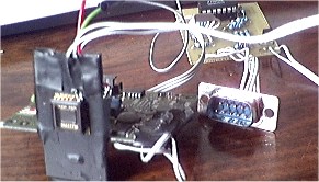
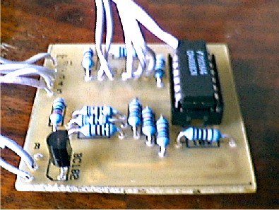
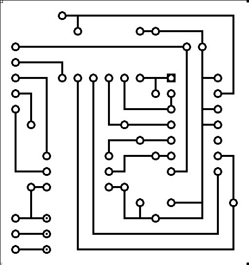
To make my life easier, and because I had the bits to do
it, I have put the circuit on a PCB. The pcb will easly
fit inside the vesta case but see next page for a much
better idea. If you would like to do the same the
graphics are below. They should be printed out at 1.6x1.7
inch. Also the Express pcb file is here.
If you will be shopping at Maplins the
codes you need are:-
QB55K for the transistor although anything similar will do.
QX23A for the 4066B.
Both are stocked at Maplin shops
Also you will need a connector for the control lines. I
have used 9 pin D connectors. 5 pin DIN or RJ45/RJ11
network type connectors would also make a good choice.
When choosing cable go for something lightweight and flexible.
Addendum.
If you are
implementing the amp switch on a ToUcam add a 420ohm
resistor between the collector and emitter of the amp
control transistor.
If the addition of
the amp switch transistor introduces diagonal banding to
the images try either shortening the leads to the ccd
from the transistor; or adding a 10uf capacitor again
between the collector and emitter of the amp control
transistor.
For more information
on amp switching please follow these links.
William
Behrens
Martin Burri
Peter Katreniak
Mike
Kudenov
|


